
Prof. Dr. rer. nat. Benjamin Butz
Head of research group
Head of Micro- and Nanoanalytics Facility (MNaF)
https://www.uni-siegen.de/nt/service/geraetezentrum
Room: PB-A 218/219
Phone: +49 271 740-3175
Fax: +49 271 740-2545
Em@il: benjamin.butz(at)uni-siegen.de
Web: Researchgate
Web: Publons
Address
Universität Siegen
Department Maschinenbau
Research Group for Micro- and Nanoanalytics
Paul-Bonatz-Strasse 9-11
57076 Siegen
Benjamin Butz was born in Otterstadt (south Germany) in 1978. He received his diploma in physics from the University of Karlsruhe (TH) in 2004. Focus of his diploma thesis as well as of his doctorate in Prof. Dagmar Gerthsen’s group (Laboratory of Electron Microscopy, KIT) was the application of advanced TEM techniques to clarify inherent degradation phenomena of functional zirconia ceramics for fuel cells. In 2010, he joined the young group of Prof. Erdmann Spiecker at the FAU Erlangen-Nuremberg, where he assisted to successfully establish advanced EM methodology and in situ capabilities for materials science and where he entered new research fields on 2D-materials and nanostructured/-particulated materials. During his research stay in Prof. Robert Sinclair’s group at Stanford University in 2016/2017 (DFG fellowship), he utilized novel in situ techniques like environmental TEM for materials research. In October 2017, he was appointed professor at the mechanical engineering department of the University of Siegen, where he applies advanced SEM, TEM and ion microscopy to investigate the local (micro-)structure and chemistry of applied and novel materials down to the atomic scale. Aim of such studies is to use that knowledge to understand and optimize the material’s properties, fabrication and application.
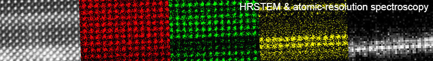
Since 2017, he has been setting up a new chair on advanced micro- and nanoanalytics at the University of Siegen with emphasis on the characterization of highly reactive materials and devices. The group’s independent research includes the development of novel in situ techniques as well as materials research on 2D semiconductors and energy materials.
Aktualisiert um 1:46 pm am December 30, 2019 von Benjamin Butz
