
2D Semiconductors
2D materials have gained significant scientific and industrial attention since the demonstration of the novel properties of graphene. Different synthesis and assembly routes allow us to study novel inherent material’s characteristics [1, 2] as well as to tailor properties for a range of applications such as sensors or photodetectors [3-5]. Through highly interdisciplinary collaborations, we employ various syntheses including micromechanical and electrochemical exfoliation as well as thermally facilitated growth techniques. Our research fields are:
- Mono-/bi-/few-layer 2D (semi)conductors with defined properties
- Scale-bridge investigation of properties and defects (OM, Raman (micro)spectroscopy, SEM & TEM)
- Material integration into devices and testing for novel properties
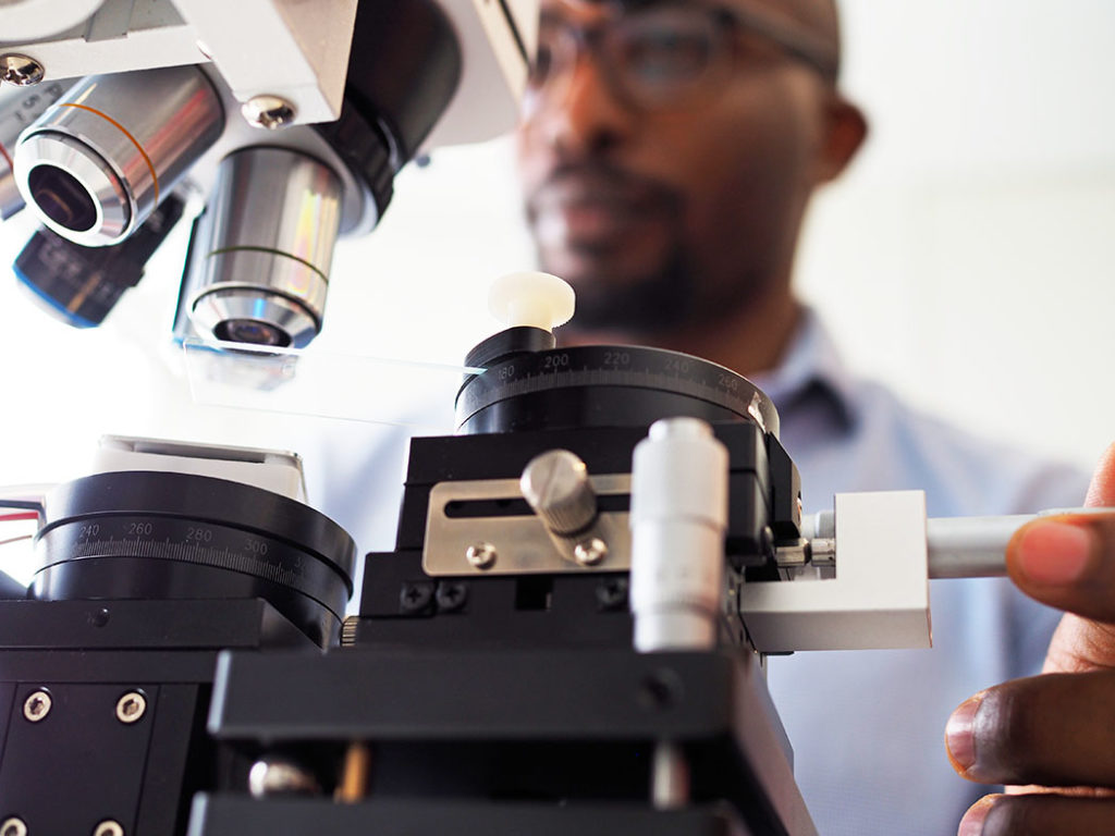
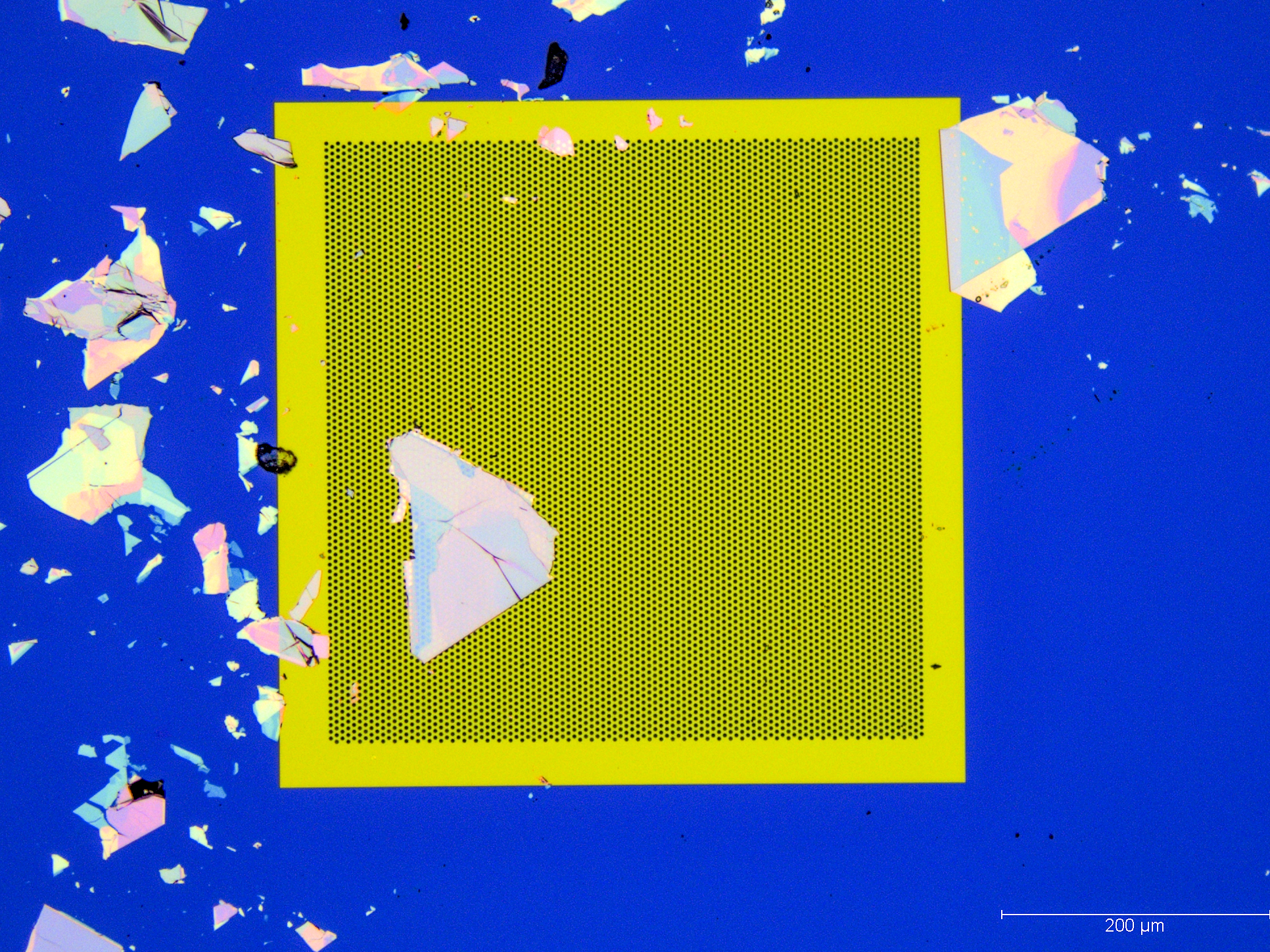
For mechanical exfoliation and device assembly, we utilize an advanced setup for dry stamping (see picture gallery, LMN equipment). Currently, we are developing an automated exfoliation tool to enhance the reliability of the mechanical procedure and the quality of the obtained 2D crystals.
Dry transfer 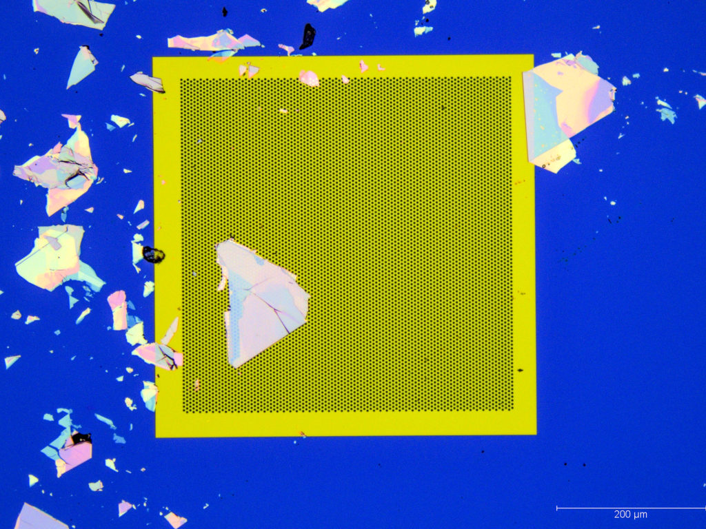
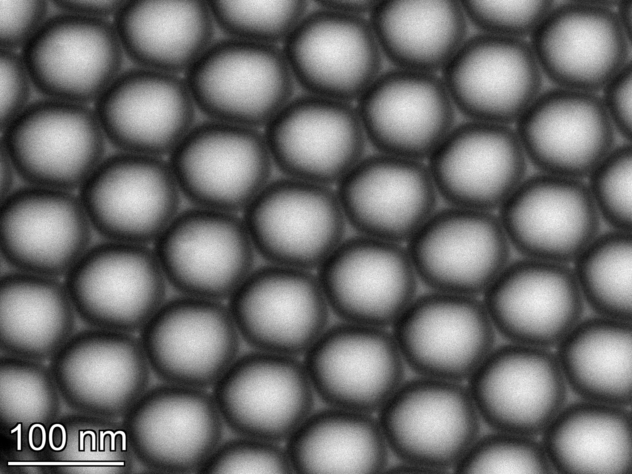
MoS2 flakes on silicon nitride TEM grid 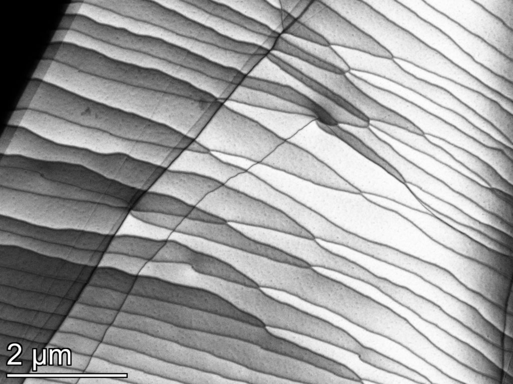
Dislocation network on MoS2 
Hexagonal defect features on MoS2 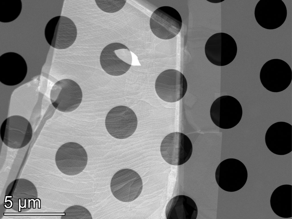
Multiple defect features on MoS2 
HRTEM image of SnS2 
Device integration [4] 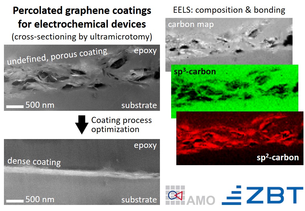
Microstructure of Graphene Coating


Students and collaboration partners are highly welcome! Contacts: Charles Ogolla, Dr.-Ing. Julian Müller, Prof. Dr. Benjamin Butz
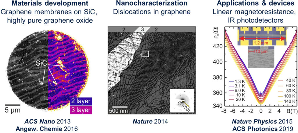
[1] B. Butz, C. Dolle, F. Niekiel, K. Weber, D. Waldmann, H.B. Weber, B. Meyer and E. Spiecker
Dislocations in bilayer graphene
Nature 2014, 505, 533
[2] B. Butz, C. Dolle, C.E. Halbig, E. Spiecker and S. Eigler
Highly Intact and Pure Oxo‐Functionalized Graphene: Synthesis and Electron‐Beam‐Induced Reduction
Angewandte Chemie 2016, 55, 15771-15774
[3] F. Kisslinger, C. Ott, C. Heide, E. Kampert, B. Butz, E. Spiecker, S. Shallcross and H.B. Weber
Linear magnetoresistance in mosaic-like bilayer graphene
Nature Physics 2015, 11, 650-653
[4] A. Bablich, D.S. Schneider, P. Kienitz, S. Kataria, S. Wagner, C. Yim, N. McEvoy, O. Engstrom, J. Müller, Y. Sakalli, B.Butz, G.S. Duesberg, P.H. Bolívar and M.C. Lemme
Few-layer MoS2/a-Si: H heterojunction pin-photodiodes for extended infrared detection
ACS Photonics 2019, 6, 1372-1378
[5] D. Waldmann, B. Butz, S. Bauer, J.M. Englert, J. Jobst, K. Ullmann, F. Fromm, M. Ammon, M. Enzelberger, A. Hirsch, S. Maier, P.Schmuki, T.Seyller, E. Spiecker and H.B. Weber.
Robust graphene membranes in a silicon carbide frame
ACS Nano 2013, 7, 4441-4448
Aktualisiert um 12:47 pm am July 16, 2020 von Benjamin Butz
