
Micro- and Nanoanalytics Group » in situ Electron microscopy
in situ Electron microscopy
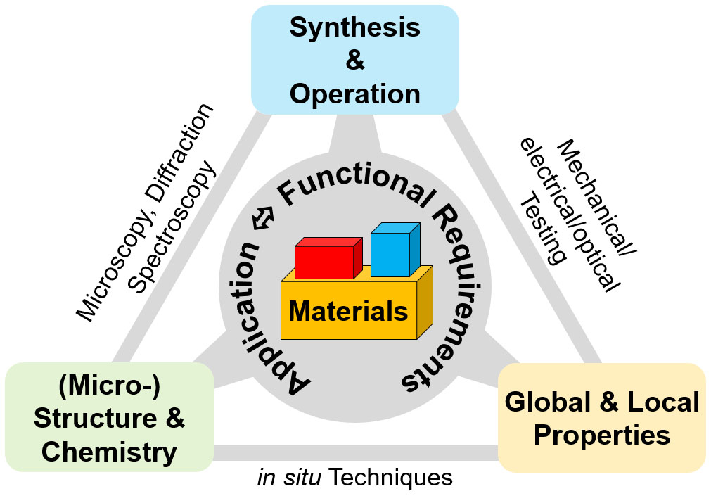
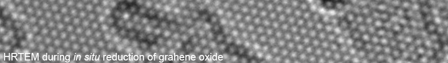
Our group employs and develops in situ/in operando SEM and TEM techniques and devices to solve materials issues. With planned purchases, the methodical portfolio will range from heating (plus biasing) to environmental to mechanical testing within the SEM and TEM. Recent studies:
Batteries, fuel cells and related
- Li et al, Nano Lett. (2017), 10.1021/acs.nanolett.7b02630
- Li at al, Science (2017) 10.1126/science.aam6014
- Butz et al, SSI (2006) 10.1016/j.ssi.2006.09.003
- Niekiel et al, Ultramicroscopy (2017) 10.1016/j.ultramic.2016.11.028
Structure formation & Phase transformations
- Butz et al, Angew. Chem. (2016) 10.1002/anie.201608377
- Niekiel et al, Acta Mater. (2016) 10.1016/j.actamat.2016.05.026
- Birajdar et al, Scripta Mater. (2012) 10.1016/j.scriptamat.2011.12.045
- Ran et al, Nanotechnology (2016) 10.1088/0957-4484/27/42/425703
Failure
- Roy et al, Acta Mater. (2010) 10.1016/j.actamat.2009.12.015
Latest in situ development
- Development (in close collaboration with the Lehrstuhl für Umformtechnik, UTS) of miniaturized bending machine for in situ studies of phase transformations, crack initiation and growth: 3-point bending geometry to ensure most constant sample height; compatible with FEI Helios 600 FIB/SEM allowing for in situ imaging and crystallographic investigation by EBSD (support by Mr. Weiß, Kammrath & Weiss GmbH gratefully acknowledged)
- Basic specs: max. load 4 kN, bending radius 1 mm, force & displacement measurement, dimensions 100 x 100 x 50 mm3, mass 700 g, sample dimensions 20 x 3.5 x 2 mm3
- Contacts: Matthias Weber, Rainer Steinheimer (UTS), Benjamin Butz
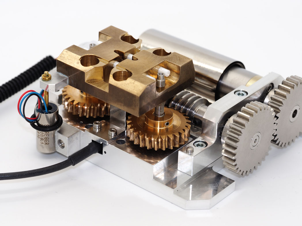 |
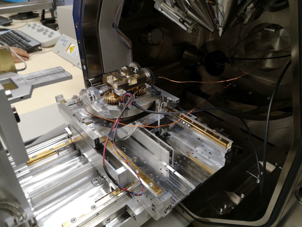
in situ bening in FIB/SEM 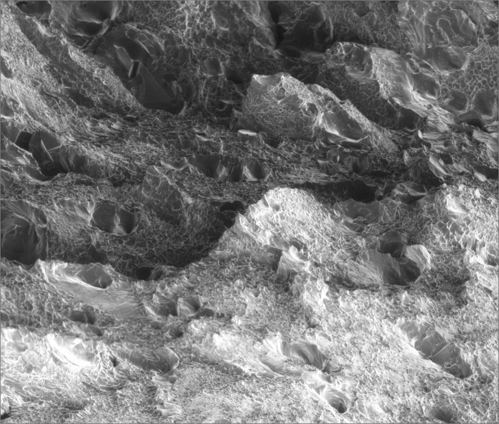
SEM of fracture surface
Aktualisiert um 5:15 pm am September 22, 2023 von Benjamin Butz
